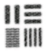
Readout of GEM detectors
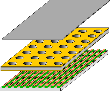
One or more Gas Electron Multiplier electrodes are used to amplify the primary charge in avalanche and transfer a large fraction of the avalanche electrons to a signal induction gap. We have developed various schemes for one- and two-dimensional localization using as charge collection electrodes various projective patterns realized with the metal-insulator etching technology developed at CERN for manufacturing the GEM electrodes. The major advantage of this approach is that both coordinates are read-out at ground potential, thus avoiding the need of bulky and potentially unreliable HV capacitors necessary in other schemes. Moreover, the global (positive) signal detected on the lower GEM electrode can be used for trigger or energy selection. To obtain larger gains, a multiple GEM structure can be used.
Schematics of the GEM detector with 2-D readout. Electrons transferred from the avalanche in GEM are collected by the pick-up electrode. This consists in one set of parallel metal strips sitting on thin kapton ridges, and a second set of perpendicular metal strips on the bottom of the ridge. The collected charge is shared between strips in the two layers; a center-of-gravity calculation provides the central avalanche coordinate in two projections:
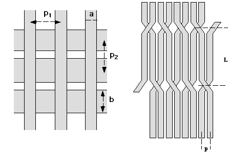
Examples of projective read-out patterns: carthesian and small-angle stereo. The strips’width can be adjusted to have equal sharing of collected charge:
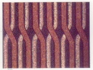
Micro-photograph of a cartesian 2-D readout pattern. The distance between strips is 200 µm, and the strip width 50 ans 150 µm on the top and bottom layer respectively. The kapton ridge separating the two layers is 25 or 50 µm thick:
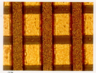
NOTE: With the geometry shown, the charge sharing is not equal between coordinates (~50% larger charge on top layer). This can be corrected making the top strips narrower (but they would be rather delicate).
In the COMPASS chambers, with a pitch of 400 µm, a strip width of 80 and, respectively 340 µm provides equal charge sharing (see COMPASS)
Micro-photograph of a small-angle stereo readout pattern, in the region of crossing between the two layers of strips (separated by 25 µm thick kapton ridges):
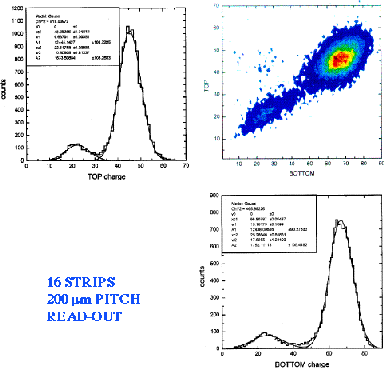
Pulse height spectra recorded irradiating the detector with 5.9 keV X-rays (gas filling: argon-carbon dioxide). The charge recorded on 16 adjacent strips in two perpendicular projections is shown, as well as their two-dimensional correlation:
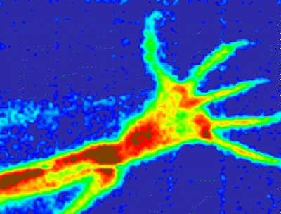
8 keV X-ray absorption radiography of a micro-mammal detail (the foot of a bat). The real image size is ~11×9 mm2:
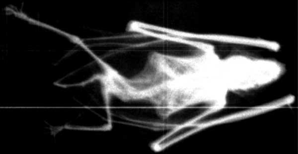
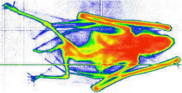
8 keV X-ray “full body” absorption radiography of a micro-mammal (a bat). Image size ~ 6 cm x 3.5 cm)
False color representation of the same image:
PAD READOUT
For very high rate operation or special applications (for example Time Projection Chambers) the readout board can be patterned with pads, with a size adjusted to the experiemtal needs, and individually read-out. For high rate detection of photons, this is the only way to avoid the ambiguities arising from multiple simultaneous events in projective strip readout.
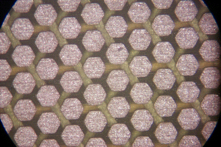
A way to preserve multi-track capability with a considerably smaller number of readout channels is the so-called “Hexaboard”, a pattern of hexagonal pads interconnected by strips on the back plane along three directions at 60 degrees. The multi-layer interconnection technology has been developed at CERN’s printed circuit workshop
Close view of the Hexaboard:
Example of two-dimensional X-ray absorption pattern through a mask, 1 mm on the side, reconstructed from the three projections in the hexaboard chamber. Left: original (low rate) image; center: the same obtained adding by software pairs of events; right: adding three events.
