GEM developments
Minimising parallax-broadening with a planispherical GEM
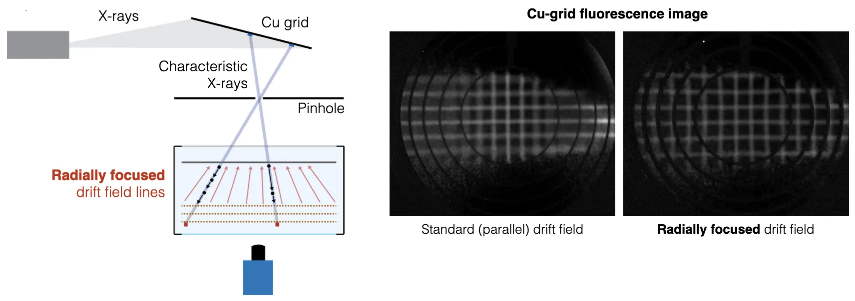
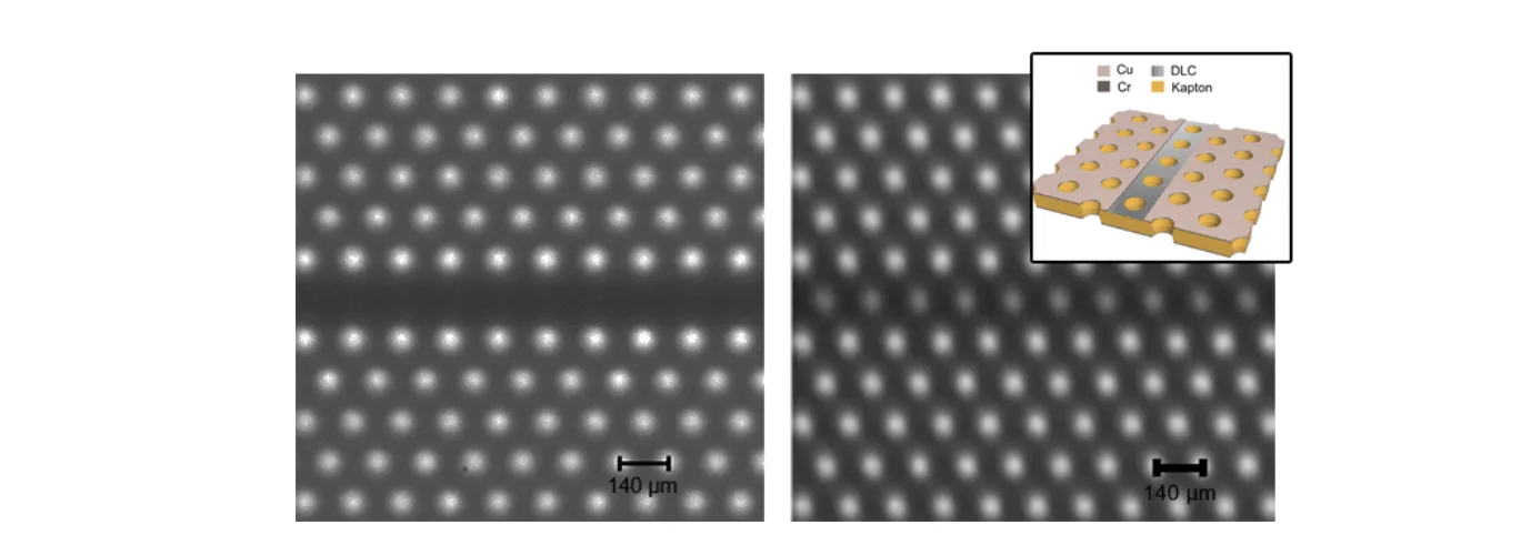
Minimising distortions from segmented GEM electrodes
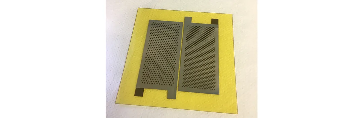
Large-area Gaseous Electron Multiplier (GEM) electrodes are by default segmented to decrease the capacitance of the foils and consequently minimise the released energy in the event of discharges. Sectors are typically created by removing one row of GEM holes and separating the electrodes by a thin insulating gap. However, this segmentation results in distortions of the electric field and of the response of the detector in the vicinity of the blank gaps between sectors as shown in the left image.
To recover the response in the sector gaps and minimise distortions, we studied several designs of sector gaps with GEM holes in the insulating region as well as a sector gap coated with a resistive Diamond-Like Carbon (DLC) layer, as shown in the inset on the right. The right image shows the response of a segmented GEM with a DLC layer and holes in the sector gap. The response of the holes in the sector gap is recovered and distortions in the resulting images are reduced. The resistive DLC layer in the gap between sectors reduces distortions while maintaining the protective effect of segmented electrodes for large-area GEM-based detectors.
A.P. Marques et al. Minimizing distortions with sectored GEM electrodes, NIM A, 2020
3D printed THGEM
Additive manufacturing techniques offer unprecedented flexibility and are already widely used for intricate mechanical structures. Employing a novel inkjet-based 3D printing technology combining insulating and electrically conductive materials, we investigated the applicability of this manufacturing approach for detector development.
High-resolution inkjet 3D printing was used to develop a fully printed Thick Gaseous Electron Multiplier (THGEM) as shown in the right figure above. The printed device was operated as a gaseous detector, thus proving the possibility to 3D print functional radiation detectors. While the achievable resolution cannot compete with photolithographic techniques, inkjet 3D printing offers significantly higher geometrical flexibility and shorter prototyping times, potentially enabling result-driven detector development and optimization and evaluation of non-planar structures.
F.M. Brunbauer et al. 3D printing of gaseous radiation detectors, JINST, 2019